


What Our Users Say
Through INUP-i2i, the exposure and research environment at IIT Guwahati significantly contributed to my overall professional development and helped shape my academic and personal growth.
I have learned about a lot about lithographic and growth tools during the hands-on training at CeNSE IISc Bangalore. We couldn't get the success in our project with INUP due to some restriction on growing the magnetic materials inside the cleanroom. However, after learning from INUP programme, I have independently operated these tools at NRF, IIT Delhi and National University of Singapore and published high-impact papers during my PhD and postdoc.
The INUP program provided a great opportunity to explore advanced fabrication and characterization techniques within the research environment at IIT Bombay. These facilities are a boon for researchers from institutes with limited resources. The results obtained during my project under INUP were instrumental in finalizing my PhD thesis. I am deeply grateful for the support and guidance provided throughout the project.
INUP is totally free workshop for the researchers community with a world class facilities to boost their research work. All the raw materials are generally obtained from the INUP facility itself. Familiarisation is the first step, followed by hands-on training and then a research proposal can be submitted after that and project can be availed based on the scrutiny.
The workshop was beneficial for students pursuing nanotechnology-based degrees. It also forms the base for people interested in the fabrication field of devices. I believe it is a great initiative by IIT-Delhi to train the youth in fabrication technology making them ready for the future of semiconductor technology in India.
INUP-IIT Madras has played a pivotal role in my research by offering cutting-edge infrastructure, training programs, and collaborative opportunities in nanoelectronics and advanced materials research. We extend our heartfelt gratitude to the INUP program funded by MeitY, GOI.
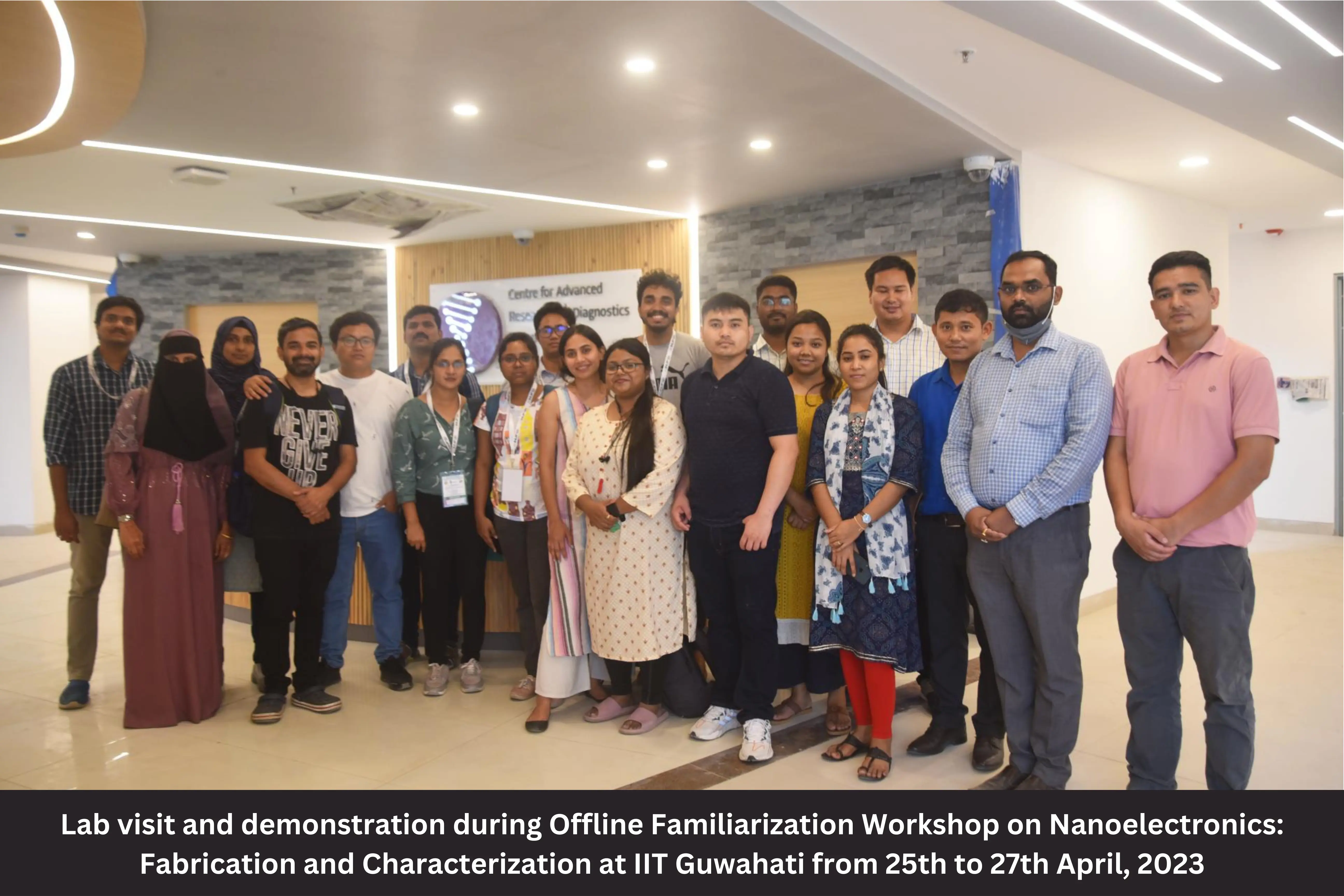
The INUP program provided hands-on training in various advanced technologies, access to laboratory facilities, and a supportive research environment. The staff at CFN, IITG were very friendly and helpful.
The INUP program provided me with an incredible opportunity to enhance the outcomes of my research by granting access to state-of-the-art facilities. These advanced research facilities played a crucial role in refining my experiments and achieving more precise and impactful results. Moreover, it gave me a new level of confidence to pursue my journey from Sharda University to IISc, which has been nothing short of a "dare to dream" moment. This project has opened numerous avenues for me, shaping my academic and professional aspirations.
Utilizing INUP facilities since my PhD has been crucial in completing my research without deviation, especially since my home institute lacked sophisticated fabrication and testing equipment. This support directly enabled me to secure a National Post-Doctoral Fellowship and continue my research through an SERB fellowship. Such programs are essential for advancing "Make in India" initiatives and competing globally in semiconductor technology.
INUP is a central facility under indian nano-electronics users program and provides very advanced research facilities for the betterment of the students. INUP is basically allotted to 6 institutes in the countries. The new thing or fact which I learned was, It is totally free and it also provides the raw materials to the users who avail their facilities.
Thank you for the great course. Great presentation style with lots of opportunities to ask questions and talk about real life examples which all made for a really enjoyable and informative course. This has more than met my expectations. A wonderfully practical course - both personally and professionally.
With the lithographic and material characterization support from INUP at CNNP, IIT Madras we are working on fabricating substrates for milk adulteration detection. We express our gratitude to the Indian Nanoelectronics Users Program INUP @ IIT Madras supported by MeitY GOI.
Through INUP program, we could able to do a few experiments on the planned research problem which was not possible without the facilities provided by CFN, IITG.
Very happy to express my deepest gratitude to CENSE INUP in helping me complete my Ph.D research work, because of which I'm in this position( Incharge of Physics Dept.- HOD)
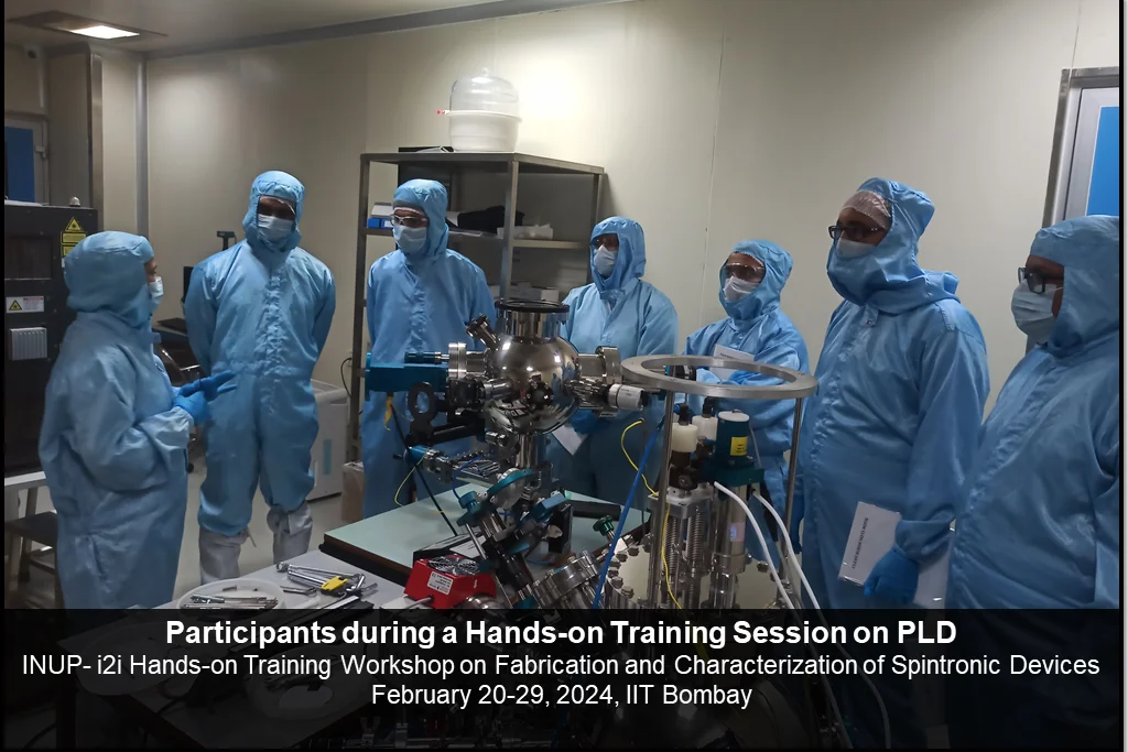
The INUP program provided essential hands-on training in advanced oxidation and lithography techniques, as well as 4-probe characterization measurements. We are sincerely grateful to the INUP and IITBNF lab members for their dedicated efforts in explaining the integration processes and standard operating procedures (SOPs) for fabrication and characterization. This expert guidance was instrumental in helping us master complex technical workflows.

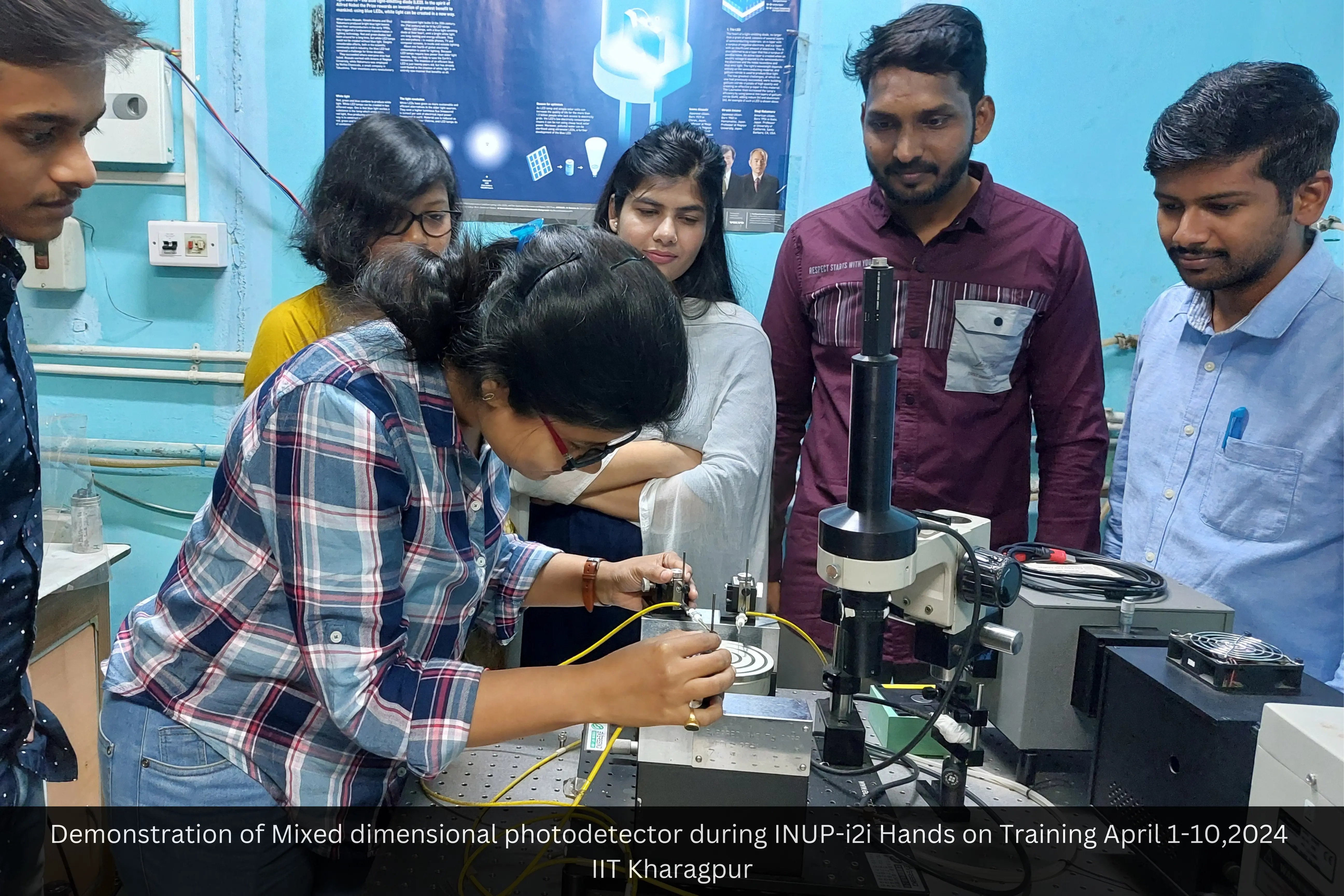
I learned various advanced techniques in nanofabrication, such as electron-beam lithography, atomic layer deposition, and nanoimprint lithography. I also gained insights into cutting-edge characterization techniques like scanning electron microscopy (SEM),atomic force microscopy (AFM), and X-ray diffraction (XRD). These methods play a critical role in the fabrication and analysis of nanomaterials, and I now have a deeper understanding of how these techniques are applied to create and study nanoscale structures.
The program provided excellent learning experience, offering valuable insights into the finer details of device fabrication. It also served as a strong platform for discussing and sharing research ideas and challenge.
We carried out our R&D work including fabrication and characterization of perovskite solar cell devices at the INUP-IIT Madras during my PhD at Amrita Vishwa Vidyapeetham. I am thankful for this support provided by the CNNP lab through INUP program.
INUP-i2i and the facilities at CFN, IITG helped me to complete my PhD research work and the results were published in Chemistry A European Journal.
I am currently pursuing a Ph.D. in Physics at the Department of Physics, Pondicherry University. As an INUP project fellow at CeNSE., IISc, I have had the privilege of conducting a part of my research under the C-DNA program. I have published five research articles in international peer-reviewed journals and have been honoured with several awards for best research presentations. At present, I am deeply engaged in writing my doctoral thesis and am actively exploring opportunities to pursue postdoctoral research in my field.
As a proud INUP user, I completed seven projects focusing on resistive RAM research, benefiting from world-class fabrication and characterization facilities. The program’s disciplined, systematic approach and expert mentorship from INUP staff members and mentors respectively led to nine publications, ten conference presentations, and prizes. This transformative experience even resulted in a nomination for the best PhD thesis award at the DAE symposium at BARC.
Had a great experience of learning from some of the best of the field. From flexible devices, sensor application, laboratories to battery application, the workshop is overall very useful for young researchers. Looking forward to collaborate with IIT Kharagpur.
The hands-on training in semiconductor device fabrication, along with visits to advanced nano research facilities, provided valuable practical exposure to cutting-edge technologies. The strong focus on fabrication and characterization techniques—particularly e-beam deposition, lithography, and sputtering—greatly enhanced the learning experience. Exposure to cleanroom operations was especially insightful, making the programme highly relevant and impactful for researchers in nanoelectronics and semiconductor technology.

We extend our heartfelt gratitude to INUP-IIT Madras for their unwavering support. Their provision of the state-of-the-art fabrication and characterization facilities at the Centre of NEMS and Nanophotonics (CNNP) has been instrumental in our research journey. This achievement not only reflects our commitment to pushing the boundaries of nanoelectronics but also underscores the collaborative spirit of academic research in India.
While cleanroom concepts are often confined to textbooks, the INUP workshops and hands-on sessions enabled me to work confidently in a real cleanroom environment at CFN, IITG and understand fabrication workflows. I was awarded the ISSS Postgraduate Student Award 2024 (Runner-up) and also received the Best Thesis Award at NIT Silchar.
The execution of the project through INUP program at IISC Bangalore has helped me complete my then ongoing PhD program immensely. Also I could join IIT Guwahati as a Senior Research Fellow after the completion of the INUP project.
Joining the INUP program during my master's thesis was a transformative experience that served as a pivot for my career in semiconductor and nanotechnology. The combination of state-of-the-art facilities and expert mentorship provided a solid foundation and the confidence needed to excel in this domain. I highly recommend this exceptional program to anyone looking to realize their potential in this field.
I gained insights into various characterization techniques and methodologies essential for analyzing thin films, including their structural, optical, and surface properties. Additionally, I developed an understanding of advanced methods for thin-film deposition, such as physical and chemical vapor deposition, as well as precision patterning techniques like lithography and etching.
We have gained so much information & knowledge from this training, and it added basic & fundamental knowledge to enhance product efficiency & quality.
I would like to sincerely thank INUP-IIT Madras for all the support and assistance provided throughout my research work. The facilities and guidance were invaluable to the successful completion of my PhD.
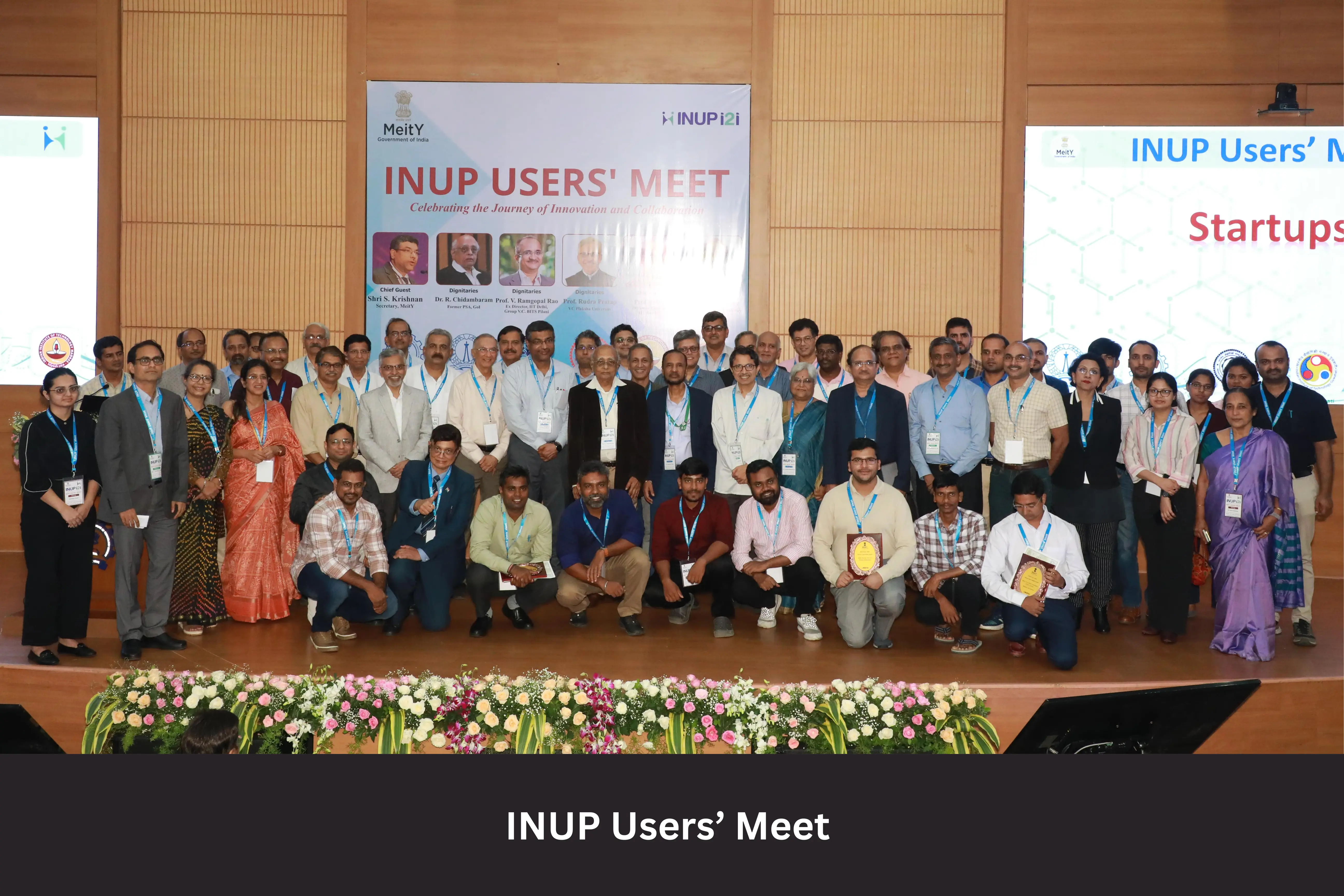
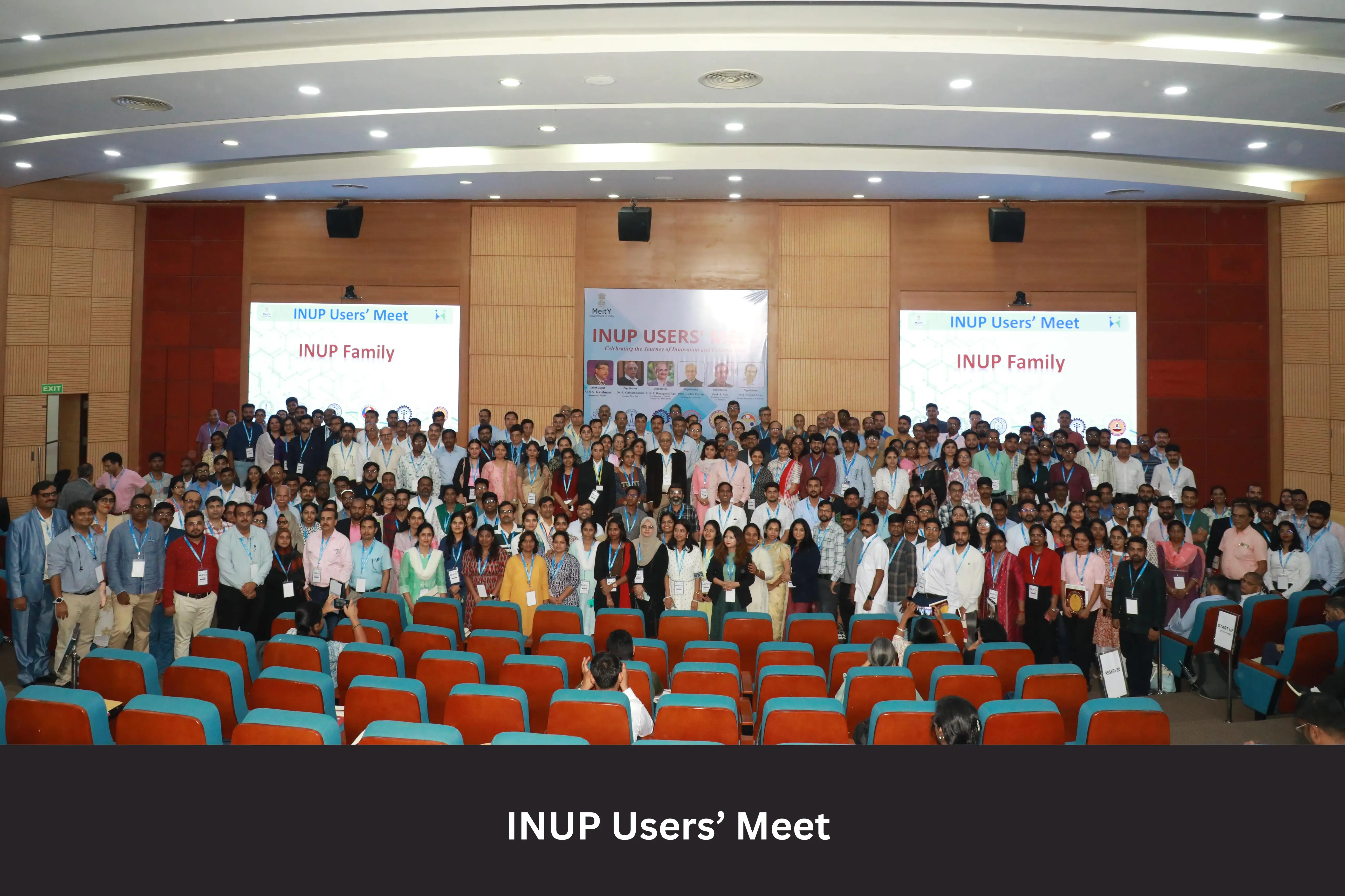
Ministry of Electronics and Information Technology – MeitY, with the long-term vision of improving skilled manpower in the areas of micro and nanoelectronics had established the Indian Nanoelectronics Users’ Programme (INUP) about a decade back. The initiative enabled the researchers to travel from the country's remotest locations and implement their ideas. The initiative enabled the researchers to travel from the country's remotest locations and implement their ideas at the state-of-art nanofabrication and characterization facilities available at Centres of Excellence established at the Indian Institute...Read More >
Participating Institutes
59
Level 1
Familiarization Workshops
46
Level 2
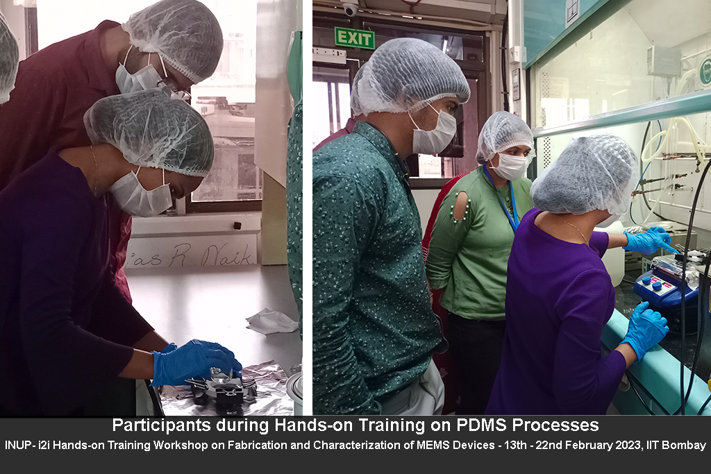
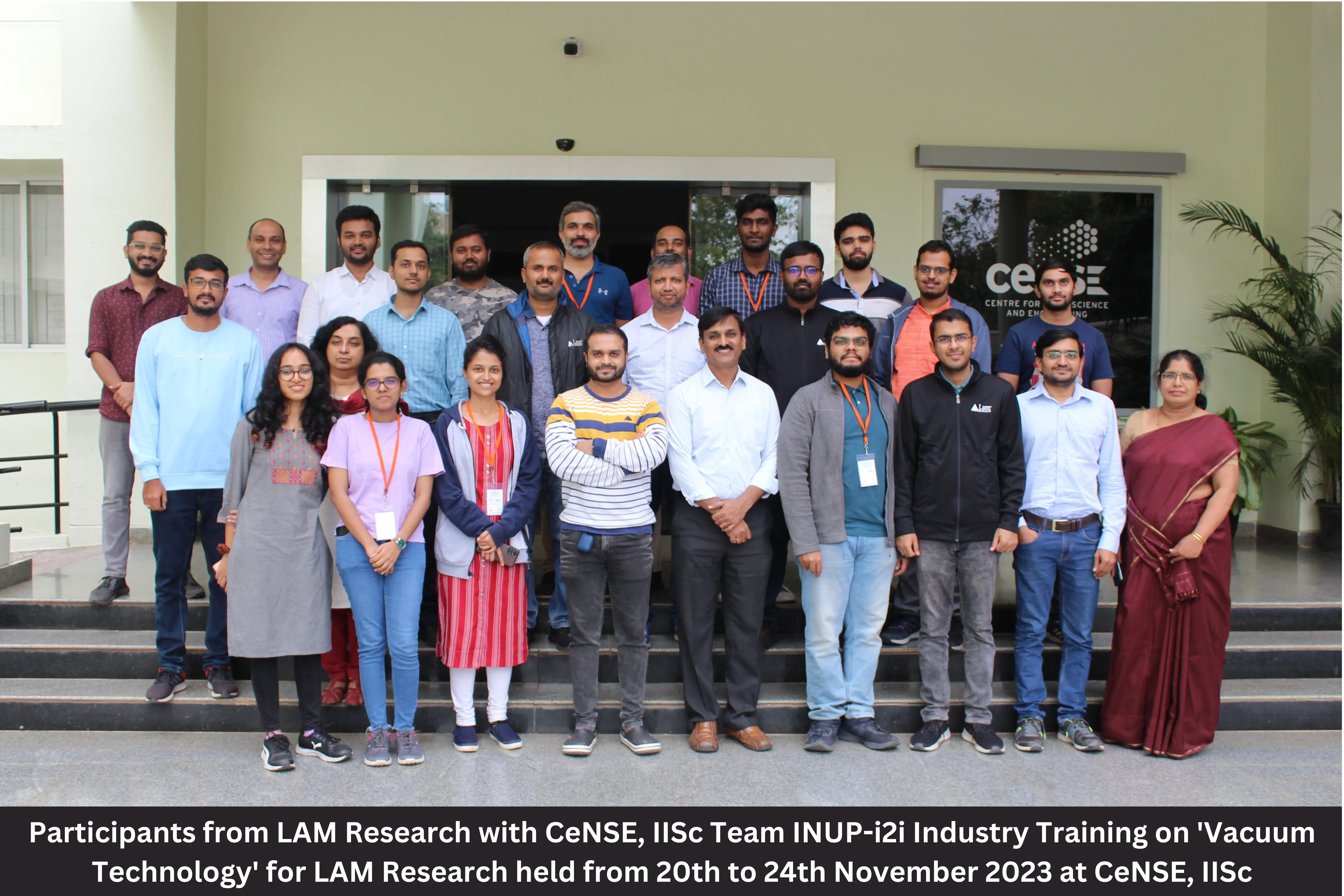
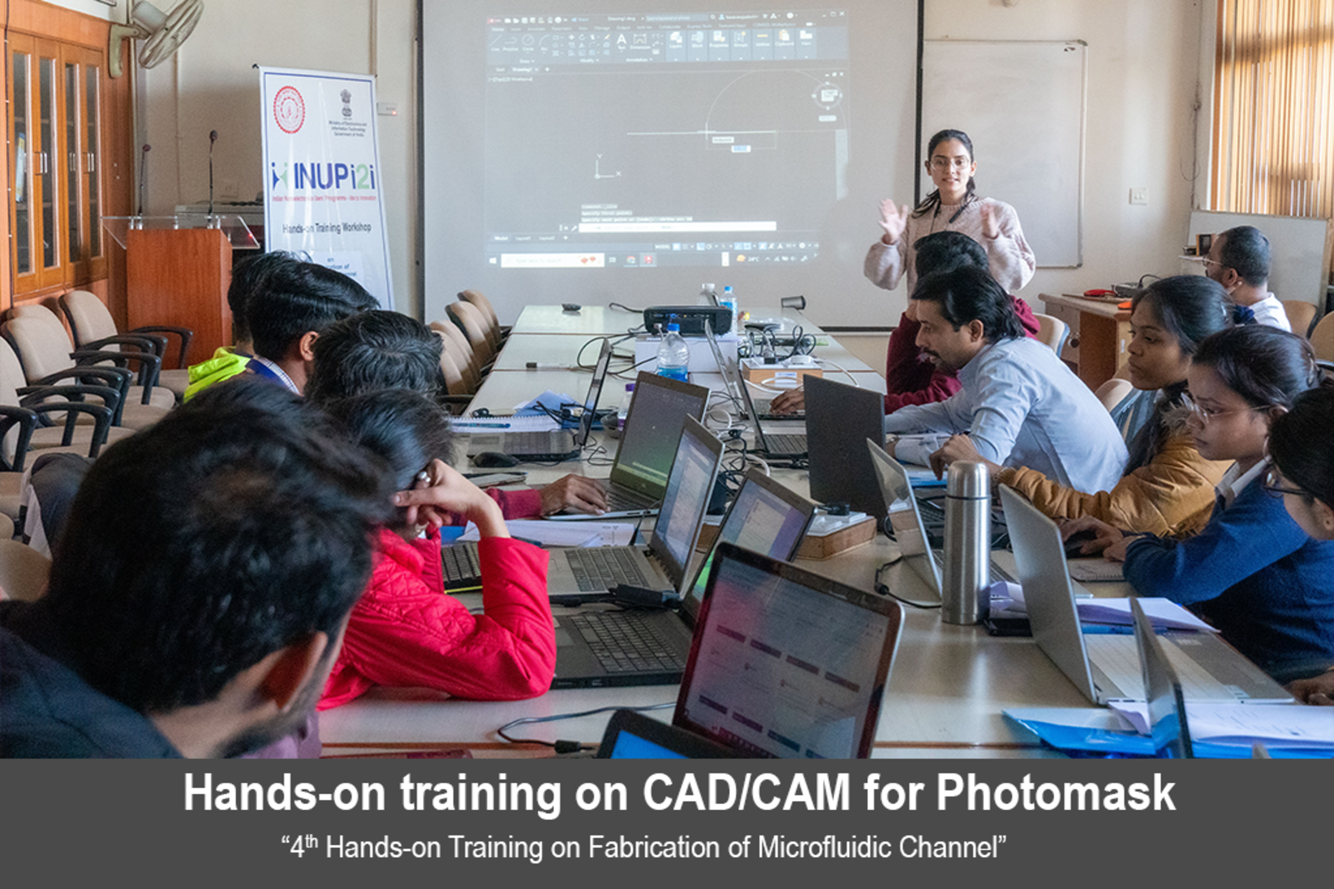
Hands-on Trainings
56
Level 3
Project Proposals Ongoing
613
Level 3
Project Proposals Completed
Statistics
Posts
Social Media Outreach